粉體行業在線展覽
粉體行業在線展覽


直接聯系
German First-Nano System 德國韋氏納米


法國
面議
946
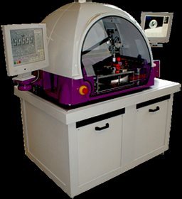
DBT1000 | DBT-1200 | ||||
Speci? cations: Die size: from 300x300μm Thickness: from 3 mil and up 2 basic con? gurations: ? Modul I : XYZ and Theta for Chip handling ? Modul II : XYZ, hi resolution, for multi chuck Shuttle and pin Test centering Z motion with adjustable angle Pickup Tool offset to Crosshair: programmable Test Pin to crosshair: programmable Joystick: proportionnal speed Chip hold on chuck by vacuum Two LCD display, used for wafer handling and for Test Monitoring. Video Target generator for alignment. Lights: Direct and pen LED lights. | Speci?cations: Die size: from 250x250μm (10mil) Thickness: from 75μm, (3 mil) and up 2 basic con? gurations: ? Modul I : XYZ and Theta for Chip handling, ? Modul II : XYZ, hi resolution, for multi chuck Shuttle and pin Test centering Z motion with adjustable angle Pickup Tool offset to Crosshair: programmable Test Pin to crosshair: programmable Joystick: proportionnal speed Chip hold on chuck by vacuum Two LCD display, used for wafer handling and for Test Monitoring. Video Target generator for alignment. Lights: Direct and pen LED lights. Facilities: Power: 100-240vac | ||||
XRD-晶向定位

CVD 真空化學氣相沉積設備
等離子體增強化學氣相沉積系統CVD
自動劃片機
BTF-1200C-RTP-CVD
Gasboard-2060
Pentagon Qlll
等離子化學氣相沉積系統-PECVD
定制-電漿輔助化學氣相沉積系統-詳情15345079037
HSE系列等離子刻蝕機